


summarize
The complexity in the IoT world is becoming more and more apparent, we recently received a request from a company to make an IoT product that monitors rats and wirelessly transmits the pictures taken, in addition to the need to monitor the environment for temperature and humidity and other commonly usedIoT SensorsOutside of that, image sensors are needed to take pictures to get information about the environment. Especially with the development of intelligent technologies like AI, we are recognizing and classifying objects with the help of machine learning concepts, all of which can be achieved with the help of image sensors.

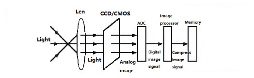
An image sensor is an electronic device that converts an optical image into an electronic signal. It is used in digital cameras and imaging devices to change light falling on the focal point of the camera or imaging device into a digital image. When light falls on the focal point of the camera, the image sensor captures the light and converts it into an electronic signature, which is then transmitted to the camera or imaging device processor, which converts the electronic signature into a digital image.
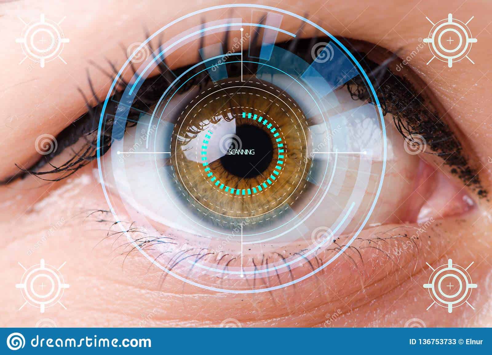
Image sensors are the biological equivalent of eyes. Image sensors make it more straightforward to capture high-quality images and video into a digital format for easy use.
In the human eye, optic rod and cone cell receptors work in concert with ganglion cells to convert photons into electrochemical signals, which can then be processed by the occipital lobe in the brain.
Sensor Classification
The basic principle of an image sensor is that photons are captured as charged electrons and silicon and converted to a voltage value through the use of capacitors and amplifiers, and then to a digital code that can be processed by a computer.
CCD (Charge Coupled Device)
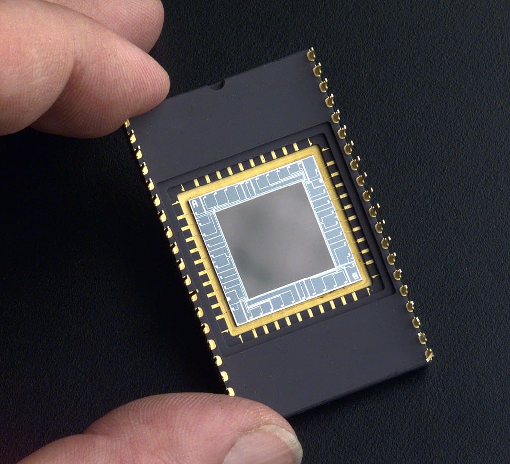
The Charge-Coupled Device (CCD) was invented in 1969 by Willard S. Boyle and George E. Smith of Bell Labs. While working on MOS technology, they realized that charge was similar to a magnetic bubble and that it could be stored on a tiny MOS capacitor. Since it was fairly simple to make a series of MOS capacitors in succession, they connected them to the right voltage so that the charge could be transferred from one to the next.The CCD is a semiconductor circuit that was later used in the first digital video camera for television broadcasting.
Early CCD sensors suffered from shutter lag. This was largely solved with the invention of the fixed photodiode (PPD), invented in 1980 by Nobukazu Teranishi, Hiromitsu Shiraki and Yasuo Ishihara of NEC. It is a photodetector structure with low hysteresis, low noise, high quantum efficiency, and low dark current.In 1987, PPDs began to be incorporated into most CCD devices as fixtures in consumer electronics camcorders and digital cameras . Since then, PPDs have been used in almost all CCD sensors and then CMOS sensors.
Each cell of a CCD image sensor is an analog device. When light hits the chip, it is held as a small charge in each photosensor. The charge in the row of pixels closest to the output amplifier (or amplifiers) is amplified and output, and then each row of pixels moves its charge one row closer to the amplifier, filling the empty row closest to the amplifier. The process is then repeated until the charges in all pixel rows have been amplified and output.
In a CCD image sensor, pixels are represented by p-doped metal oxide semiconductor (MOS) capacitors. These MOS capacitors are a fundamental part of the CCD and are biased above the inversion threshold at the start of image acquisition, allowing incident photons to be converted to electronic charges at the semiconductor oxide interface; these charges are then read out using the CCD.
CMOS (Complementary Metal Oxide Semiconductor)
Complementary metal-oxide-semiconductor (CMOS) is also an integrated array of linked or coupled capacitors. In addition, working on the same principle as a CCD, but instead of moving an electronic charge along the array and then modifying it, a CMOS sensor adds additional circuitry to each pixel, allowing it to do almost all of the individual processing of the signal before sending it directly to the CPU.

A key component of modern CMOS sensors is the pinned photodiode (PPD). It was invented in 1980 by Nobukazu Teranishi, Hiromitsu Shiraki, and Yasuo Ishihara of NEC, and then publicly reported in 1982 by Teranishi and Ishihara together with A. Kohono, E. Oda, and K. Arai, with the addition of an anti-frosting structure. The fixed photodiode is a low hysteresis, low noise, high quantum efficiency, and low dark current photodetector structure, and the new photodetector structure invented by NEC was named the "fixed photodiode" (PPD) by Kodak's BC Burkey in 1984. 1987 saw the incorporation of PPDs into most CCD sensors, which became the mainstay of consumer electronics cameras. In 1987, PPDs began to be incorporated into most CCD sensors and became the fixtures in consumer electronics video cameras, and then digital cameras. Since then, PPDs have been used in almost all CCD sensors and then CMOS sensors.
Image Sensor Parameters
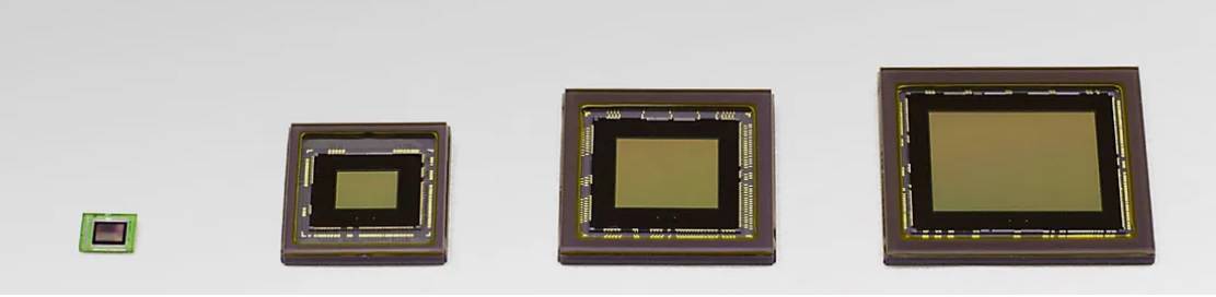
Image sensor format (size)
Image sensors come in different format types (also known as optical class, sensor size or type) and packages. The resolution and pixel size will determine the overall size of the sensor, with larger sensors having higher resolutions or larger pixel sizes than smaller sensors.
Sensor Pixel Size
Pixel size is measured in micrometers (μm) and includes the entire area of the photodiode and surrounding electronics.A CMOS pixel consists of a photodiode, an amplifier, a reset gate, a transfer gate, and a floating diffusion. Typically, a larger pixel size is better because the photodiode has more area to receive light.
(level of) sensitivity
Sensitivity is one of the important parameters of the chip, which has two physical meanings. One refers to the photoelectric conversion capability of the optical device, which has the same meaning as the response rate. That is, the chip's sensitivity refers to a certain spectral range, the unit exposure of the output signal voltage (current), the unit can be nanoampere / lux nA / Lux, volts / watt (V / W), volts / lux (V / Lux), volts / lumens (V / lm). The other refers to the radiant power (or illuminance) to earth that the device can sense, in the same sense as detection rate,. The unit can be expressed in watts (W) or lux (Lux)
frame rate
It refers to the number of pictures recorded or played per unit of time. Continuous playback of a series of pictures will produce an animation effect, according to the human visual system, when the playback speed of the picture is greater than 15 frames / s (i.e., 15 frames), the human eye basically can not see the picture jumps; in the 24 frames / s ~ 30 frames / s (i.e., between 24 frames to 30 frames) when the phenomenon of flicker has been basically not perceptible. The number of frames per second (fps), or frame rate, indicates the number of times per second that the graphics sensor is able to update the field as it is processed. Higher frame rates result in a smoother, more realistic visual experience
Monochrome and color spectral response
Due to the physical differences between monochrome and color sensors, as well as differences between sensor manufacturers' technologies and pixel structures, different sensors will perceive light to different degrees. One way to more accurately understand a sensor's sensitivity to light is to read its spectral response map (also known as a quantum efficiency map).
signal-to-noise ratio
The signal-to-noise ratio is the ratio of the signal voltage to the noise voltage, and the unit of signal-to-noise ratio is expressed in dB. The signal-to-noise ratio given by the camera is generally the value when the AGC (Automatic Gain Control) is off, because when the AGC is on, it will boost the small signal, making the noise level increase accordingly. Typical value of the signal-to-noise ratio of 45 to 55dB, if 50dB, there is a small amount of noise in the image, but the image quality is good; if 60dB, the image quality is excellent, no noise, the larger the signal-to-noise ratio indicates that the better the control of noise!
Shutter Type
The two main types of electronic shutters are global shutters and rolling shutters. These shutter types differ in their operation and final imaging results, especially when the camera or target is in motion. Global shutter sensors are critical for imaging high-speed moving objects, and roll-up shutter sensors provide excellent sensitivity for imaging static or slow-moving objects.
Sensor Manufacturers
- Sony
- Omron (brand)
- the belt of Orion
- OmniVision
- Hamamatsu Photonics
- Canon (Japanese company)
- ON Semiconductor Manufacturing
- toshiba
- STMicroelectronics
- Nikon corporation
- PixelPlus
- Pixart
- SiliconFile
- Geco Microelectronics GalaxyCore
- MURATA
- TDK
- MORGAN
- TAIYO YUDEN
- KYOCERA
- CeramTec
Related resources
Content review.